


A Systems-Level Approach to Leakage Current Mitigation in Modern Electronics
Leakage current, the unintended flow of electrical charge through or over the surface of an insulating material, represents a persistent and escalating challenge in the design, manufacture, and operation of electronic components and systems. As technological progress drives devices toward lower operating voltages, higher component densities, and reduced power consumption, the relative impact of leakage currents on performance, reliability, and safety becomes profoundly magnified. This phenomenon is not merely a theoretical concern; it manifests as increased standby power dissipation, signal integrity degradation, accelerated component aging, and, most critically, a potential hazard to end-users. Consequently, a systematic and multi-faceted strategy for leakage current minimization is indispensable across the entire product lifecycle, from initial semiconductor fabrication to final product validation.
Fundamental Physical Origins of Parasitic Leakage
Understanding the mechanistic origins of leakage current is a prerequisite for developing effective countermeasures. Leakage is not a monolithic entity but a confluence of several distinct physical phenomena. At the semiconductor level, subthreshold leakage occurs when transistors are in their “off” state, allowing a small current to flow between the source and drain due to carrier diffusion. Gate oxide tunneling, another significant contributor, arises from the quantum mechanical tunneling of carriers through the ultra-thin insulating layer beneath the transistor gate, a problem exacerbated by the relentless scaling of process nodes. Junction leakage, caused by minority carrier diffusion and generation-recombination within depletion regions, also contributes to the overall power drain.
Beyond the chip, surface leakage currents become dominant. These are currents that flow across the surface of printed circuit boards (PCBs), connectors, and component packages due to contamination, humidity, and electrostatic field distribution. This is particularly relevant for applications operating at high voltages or in harsh environments. Insulation leakage, a critical safety-related parameter, refers to current flowing through the bulk insulation of cables, transformers, and motors. The integrity of this insulation is paramount to prevent ground faults and electric shock. A comprehensive mitigation strategy must therefore address both the intrinsic leakage within integrated circuits and the extrinsic leakage arising from the system’s construction and operating environment.
Material Science and Advanced Semiconductor Design Techniques
The frontline of the battle against leakage current is waged at the material and transistor architecture level. The selection of substrate materials with higher intrinsic resistivity can directly reduce bulk leakage. For silicon-based technologies, the use of Silicon-on-Insulator (SOI) wafers introduces a buried oxide layer that significantly diminishes junction leakage and eliminates latch-up by providing superior isolation between adjacent transistors.
At the most advanced process nodes, the traditional planar transistor has largely been supplanted by three-dimensional FinFET and Gate-All-Around (GAA) architectures. These designs provide superior electrostatic control of the channel, dramatically reducing subthreshold leakage by minimizing the influence of the drain potential on the channel when the transistor is switched off. Furthermore, the integration of high-k dielectric materials, such as hafnium-based compounds, to replace silicon dioxide has been a pivotal development. These materials allow for physically thicker gate layers that achieve the same capacitive coupling as thinner silicon dioxide, thereby drastically reducing gate tunneling currents without compromising transistor performance. The strategic application of strain engineering to enhance carrier mobility also permits operation at lower voltages, indirectly reducing leakage.
For power management and analog circuits, the use of wide-bandgap semiconductors like Silicon Carbide (SiC) and Gallium Nitride (GaN) offers inherent advantages. Their higher critical electric field strength allows for the design of components with lower on-resistance and significantly reduced leakage currents at high operating temperatures and voltages, making them ideal for automotive electronics, industrial motor drives, and high-efficiency power supplies.
Circuit-Level Strategies and Power Gating Architectures
While process technology provides the foundation, circuit design techniques offer dynamic control over leakage. Power gating is one of the most effective methods employed in digital systems-on-chip (SoCs). This technique involves using high-threshold voltage “sleep transistors” to disconnect entire blocks of logic from the power supply or ground when they are idle. By cutting off the power rail, leakage currents in the gated domain are reduced to near zero. This is ubiquitous in modern microprocessors and mobile application processors for consumer electronics and telecommunications equipment, where different cores and functional units can be independently powered down.
Multi-threshold CMOS (MTCMOS) is a design methodology that leverages power gating by strategically placing sleep transistors and using a mixture of high-threshold (low-leakage) and low-threshold (high-performance) transistors within the same circuit. Non-critical paths are implemented with high-Vt cells to minimize leakage, while low-Vt cells are reserved for timing-critical paths to maintain performance. Another technique, Body Biasing, dynamically adjusts the threshold voltage of transistors by applying a bias to the substrate or well. Reverse body bias increases Vt, thereby reducing subthreshold leakage during standby modes, while forward body bias can be applied to increase performance during active operation.
For memory arrays, which can constitute a large portion of a chip’s leakage, techniques like source biasing and the use of specialized, low-leakage retention cells are standard practice. In analog and RF circuits, careful biasing and the selection of components with lower leakage characteristics, such as junction field-effect transistors (JFETs) in input stages, are critical for maintaining signal fidelity and noise performance in sensitive applications like medical devices and aerospace avionics.
System Integration, PCB Layout, and Environmental Control
Leakage current management extends far beyond the silicon die. The physical implementation of the electronic system plays a decisive role in controlling surface and insulation leakage. PCB design is a critical factor. Utilizing boards with high Comparative Tracking Index (CTI) materials is essential for preventing conductive anodic filament (CAF) growth and surface tracking, especially in high-humidity environments common to industrial control systems and automotive under-hood applications. Conformal coatings, such as acrylic, urethane, or silicone-based materials, are extensively applied to shield PCB assemblies from moisture, dust, and ionic contamination. These coatings provide a robust barrier that dramatically increases surface insulation resistance (SIR).
Maintaining adequate creepage and clearance distances, as defined by safety standards like IEC 62368-1, is non-negotiable for preventing arcing and surface leakage between conductors at different potentials. This is particularly crucial in power supplies, lighting fixtures (e.g., LED drivers), and household appliances. The selection of passive components and connectors also matters; for instance, using Class-Y (line-bypass) capacitors with low leakage current specifications in electromagnetic interference (EMI) filters is vital for meeting safety regulations.
Environmental control within the end-product enclosure can further mitigate leakage. This includes the use of desiccants, potting compounds, and sealed housings to maintain a dry internal atmosphere, thereby preserving the surface resistivity of insulators. For office equipment and telecommunications hardware operating in varied climates, these measures are integral to long-term reliability.
The Critical Role of Precision Leakage Current Measurement
Strategies for minimization are futile without the ability to accurately measure and quantify leakage current. Precise measurement is the cornerstone of design validation, manufacturing quality control, and safety certification. The measurement principle involves applying a test voltage—typically the rated operating voltage or a higher stress voltage as per standards—across the insulation barrier of the Device Under Test (DUT) and measuring the resulting current that flows through or across its surface. This process is deceptively complex, requiring instrumentation capable of resolving currents in the microamp range while withstanding high common-mode voltages and rejecting noise.
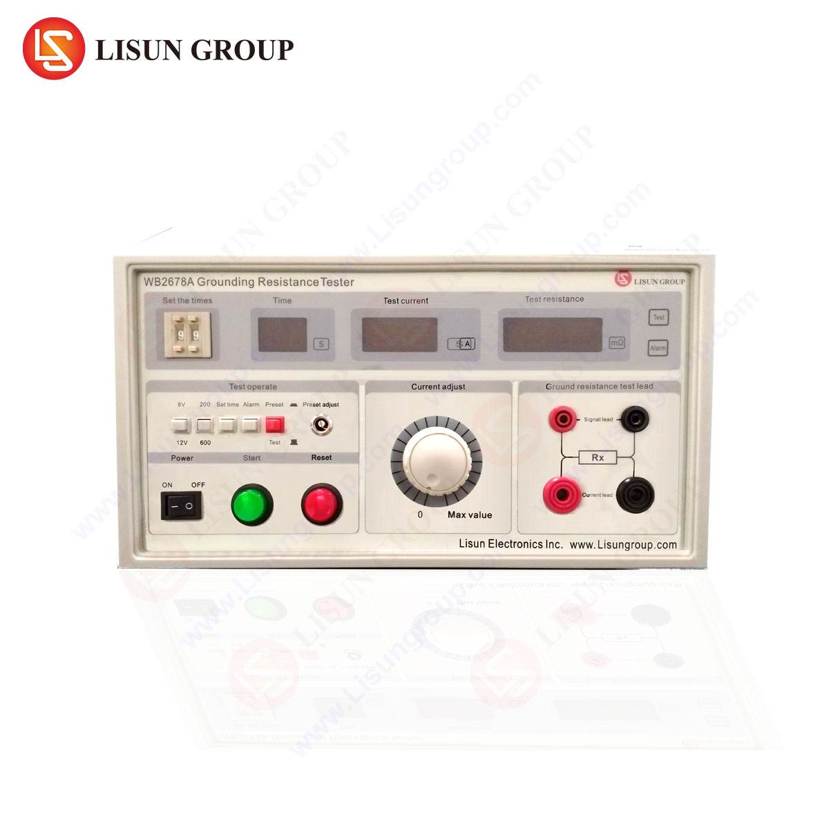
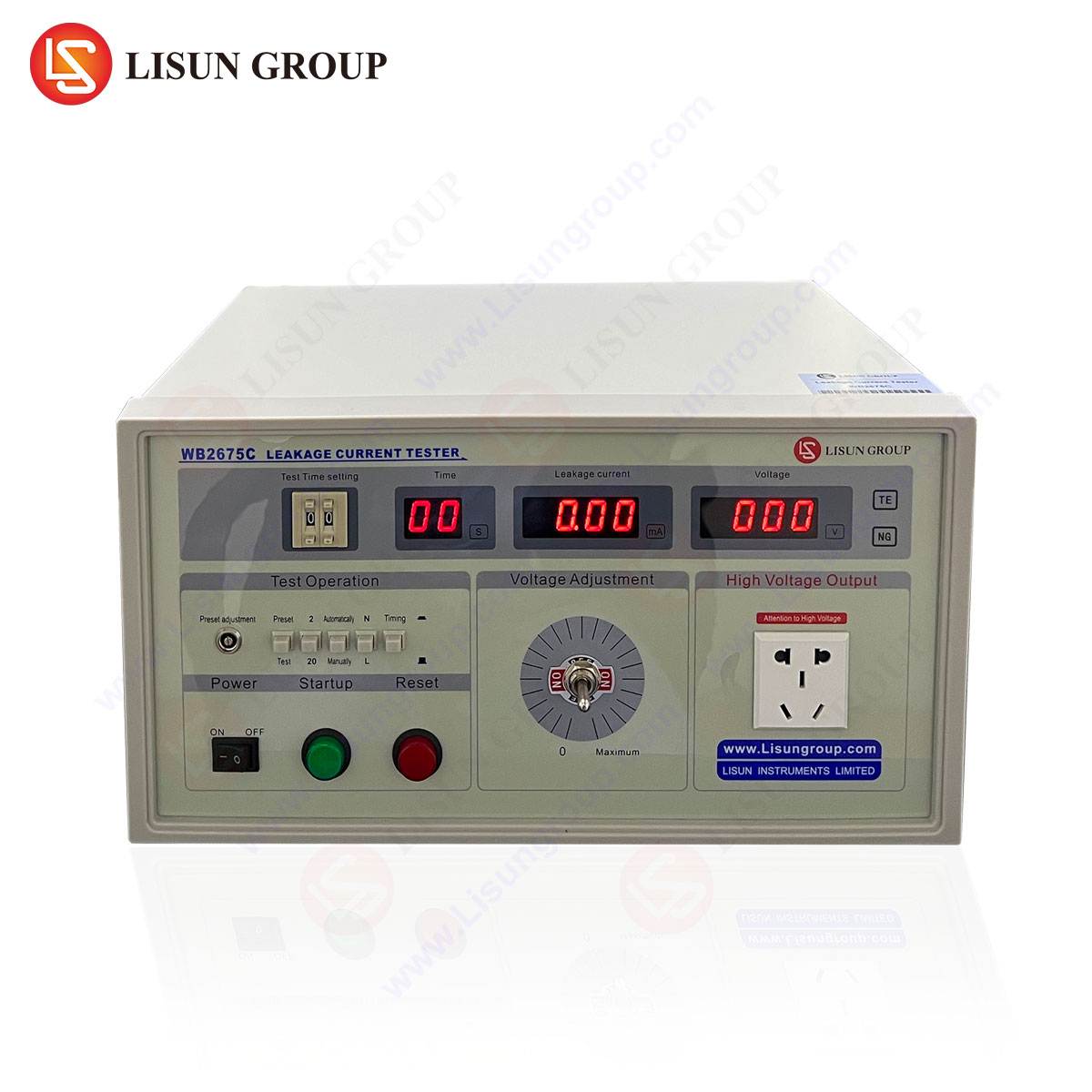
The LISUN WB2675D Leakage Current Tester is engineered to meet these exacting demands. It operates on the core principle of a precision current measurement circuit, accurately quantifying the current flowing from the live parts of the DUT to its accessible conductive parts or ground through the instrument’s internal sensing impedance. The WB2675D complies with major international standards, including IEC 62368-1, IEC 60335-1, and IEC 60601-1, making it applicable across a vast spectrum of industries.
Table 1: Key Specifications of the LISUN WB2675D Leakage Current Tester
| Parameter | Specification |
| :— | :— |
| Leakage Current Measurement Range | 0 – 2mA / 20mA |
| Measurement Accuracy | ±(2% + 5 digits) |
| Test Voltage | 0 – 250V AC/DC adjustable |
| Test Frequency | 45 – 66 Hz |
| Measurement Network | Complies with IEC 62368-1, Figure G.1 |
| Display | High-resolution LCD with digital readout |
| Safety Features | Over-current, over-voltage, and ground integrity protection |
The competitive advantage of the WB2675D lies in its robust measurement network, which accurately simulates the human body’s impedance for touch current measurements, a requirement for safety testing in household appliances, medical devices, and consumer electronics. Its programmability allows for automated test sequences in production line environments, ensuring consistent and repeatable results for components ranging from automotive control units and aerospace connectors to power supplies for lighting fixtures and industrial PLCs. By providing reliable, standards-compliant data, it enables engineers to identify insulation weaknesses, verify the efficacy of design choices, and ensure final products are safe for end-users.
Validating Mitigation Strategies Through Industry Use Cases
The practical application of these strategies, verified by precise testing, can be observed across diverse sectors. In the medical device industry, a manufacturer of patient monitors must ensure that leakage currents remain well below the stringent limits of IEC 60601-1, even under single-fault conditions. By employing power gating in their digital subsystems, using high-quality isolation transformers, and applying medical-grade conformal coatings to their PCBs, they minimize intrinsic and extrinsic leakage. Every unit is then validated on a production line using a WB2675D tester to measure both earth and patient leakage currents, guaranteeing patient safety.
In automotive electronics, a supplier developing a 48V battery management system for a hybrid electric vehicle utilizes SiC MOSFETs for their high-temperature, low-leakage characteristics. The module’s PCB is designed with extended creepage distances and manufactured from a high-CTI material to withstand the humid and contaminated environment of the vehicle. Post-assembly, the completed units undergo a dielectric strength and leakage current test with the WB2675D, applying a high DC voltage to simulate system over-voltage events and ensuring the insulation integrity of the high-voltage bus.
For a producer of industrial LED lighting fixtures, minimizing leakage to the luminaire’s chassis is critical for safety and electromagnetic compatibility (EMC). Their design incorporates a Class II (double-insulated) architecture and uses Y-capacitors with low leakage specifications in the LED driver’s input filter. During final assembly, each fixture is placed in a test jig, and the WB2675D is used to apply the rated AC voltage while measuring the leakage current from the live terminal to the earthed heatsink. This final test serves as a pass/fail criterion, preventing non-compliant products from reaching the market.
Frequently Asked Questions (FAQ)
Q1: What is the difference between measuring leakage current with a multimeter versus a dedicated tester like the WB2675D?
A standard digital multimeter (DMM) is not designed for safe or accurate leakage current measurement in this context. It lacks the standardized human-body simulation network, cannot safely handle the high common-mode voltages present during testing, and typically has insufficient resolution and accuracy in the microamp range. The WB2675D is purpose-built with these specific requirements, ensuring measurements are both safe for the operator and compliant with international safety standards.
Q2: How does the test voltage selection impact leakage current readings?
Leakage current is highly dependent on the applied voltage. Higher test voltages can stress the insulation more, potentially revealing weaknesses not apparent at the normal operating voltage. Standards often specify a test voltage, which may be the rated voltage or a multiple thereof (e.g., 1.06 times rated voltage for touch current tests). Using the WB2675D’s adjustable voltage source allows for testing under both normal and fault conditions as mandated by the relevant product safety standard.
Q3: In a manufacturing environment, what is a typical pass/fail threshold for leakage current?
The pass/fail threshold is strictly defined by the applicable safety standard for the product category. For example, IEC 62368-1 for audio/video and IT equipment specifies different limits for “ordinary” and “specially protected” equipment. IEC 60601-1 for medical devices has even stricter limits, particularly for equipment connected to a patient. The WB2675D can be programmed with these limits to provide a clear pass/fail indication, streamlining the quality control process.
Q4: Why is it necessary to test leakage current on products with functional earthing (grounding)?
Even with a functional earth connection, testing is crucial to verify that the grounding system is intact and effective. The test confirms that under normal and single-fault conditions (such as a loss of the earth connection), the leakage current that could flow through a human body remains within safe limits. It is a direct verification of the product’s fundamental safety design.